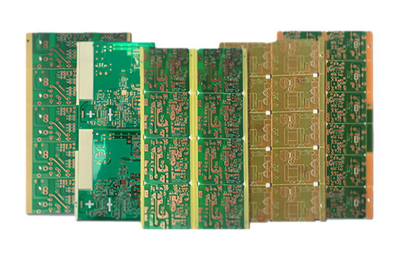
Prototype PCB service
Reduce mass production costs and eliminate pre-production issues.
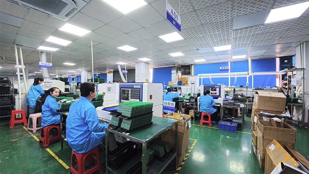
HUASUN specializes in prototype PCB manufacturing and production services, offering free DFM (Design for Manufacturability) analysis, dedicated one-on-one engineer support, flexible customization for 1 to 100 units, and 24-hour rush service to meet urgent project needs.
What is Prototype PCB ?
If you need to test whether the circuits of a newly designed PCB are properly connected and whether its dimensions match the product casing, you can simply order a Prototype PCB. In practical business operations, we recommend that you first produce a PCB prototype to validate your design. Only after confirmation that everything is correct should you proceed with prototype assembly.
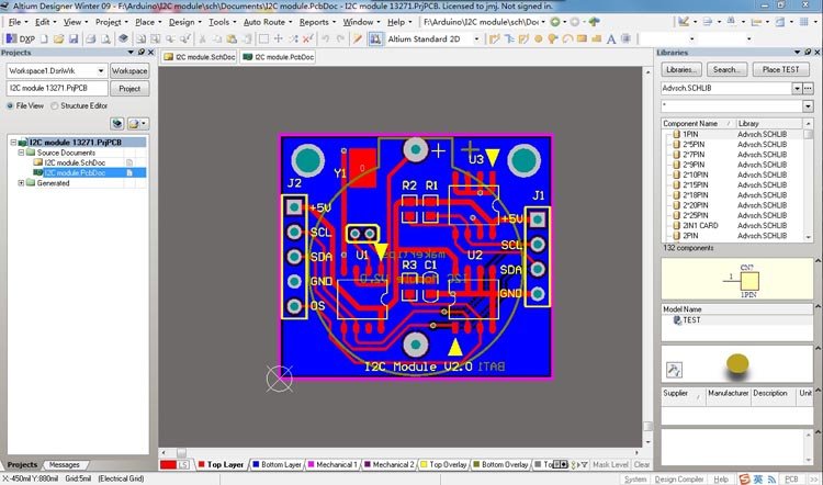
All we require from you are the PCB design files (Gerber format) and technical specifications (such as layer count, base material, surface finish, etc.), and we can then verify the electrical connectivity, structural compatibility, and manufacturing feasibility of your PCB design. This lays a solid foundation for subsequent assembly processes and constitutes an essential front-end step in the PCB manufacturing workflow.
Our Main Prototype PCB service
Fast PCB prototype
We offer 3 tiers of expedited delivery: 24-hour, 48-hour, and 72-hour turnaround. HUASUN Factory is equipped with a dedicated expedited production line to prioritize rush orders.
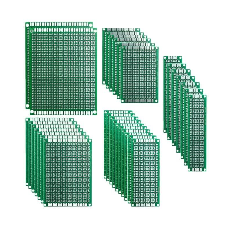
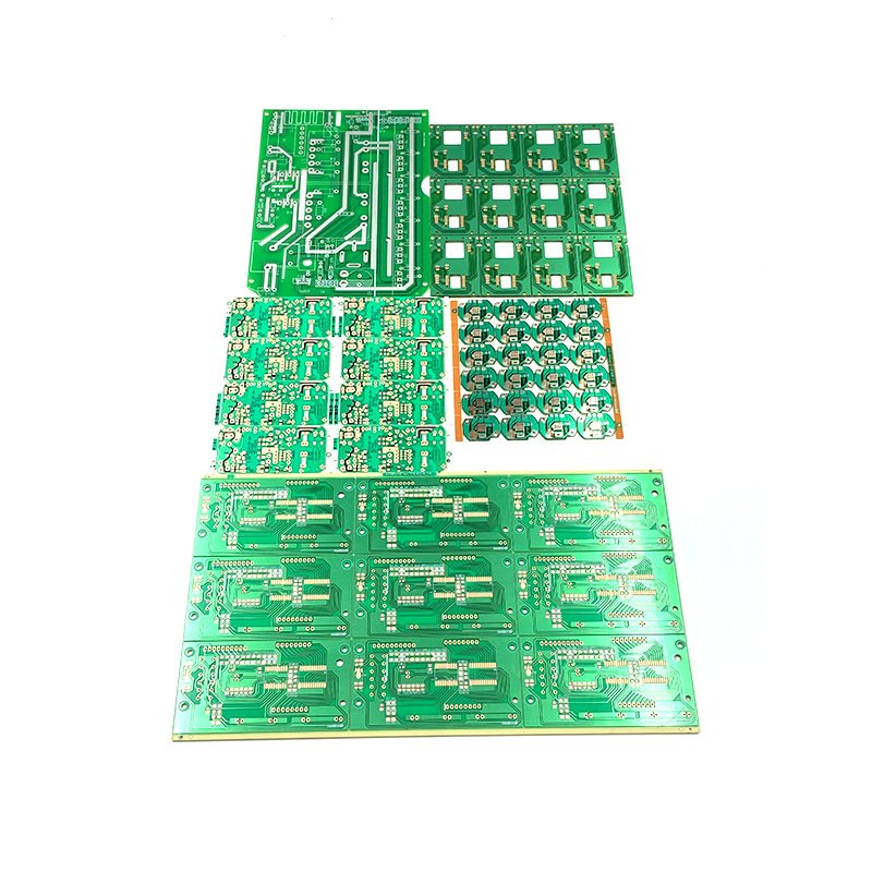
Standard PCB Prototyping
Multilayer PCB Prototyping
Specializing in high-complexity PCB prototyping, we have achieved stable production capabilities for 4-layer, 6-layer, 8-layer, 10-layer, and higher-count multilayer PCBs.
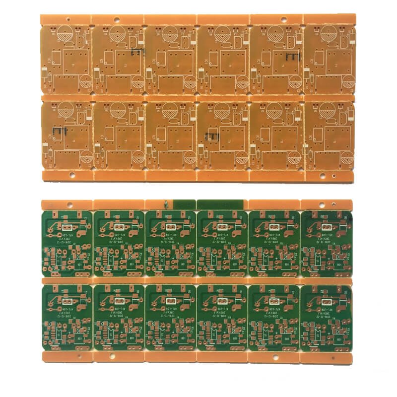
Special PCB Prototyping
Why Choose Prototype PCB Service?
Prototype PCB is primarily focused on mitigating risks, controlling costs, and accelerating R&D efficiency.
PCB design correct?
Whether there are short circuits or open circuits in the traces, the positional accuracy of pads, signal integrity, the rationality of design details, etc.
Reduce R&D costs
First, rule out PCB-specific issues,reduce unnecessary material waste at the source and lower R&D trial-and-error costs.
Verify process
Prototype PCBs help prevent issues such as low yield rates and failure to meet process standards during subsequent mass production.
Match the structure
Verify whether PCB sizes, mounting hole positions, and locating slots match the product housing and components accurately to prevent structural issues after assembly.
Shorten the R&D cycle
Why Choose US for PCB Prototyping?
————Rapid Verification of Circuit Design
- High-Precision Manufacturing Processes: Supports 0.1mm line width and spacing, 0.2mm minimum hole diameter, and circuit accuracy of ±0.02mm, fully compliant with IPC-A-600 standards.
- Versatile Material Options: Customization available for all substrate types, including standard FR-4 boards, aluminum substrates, and high-frequency boards.
- Express Delivery: 48-hour turnaround for standard prototyping, with expedited shipping available in as fast as 24 hours.
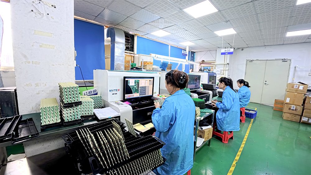
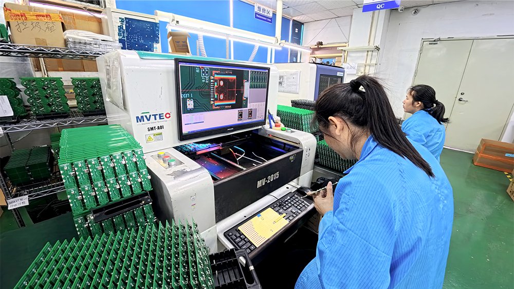
- Quality Assurance: Dual quality inspections combining AOI (Automated Optical Inspection) and flying probe testing to ensure zero defects in bare PCBs.
PCB Prototyping Process

1. Customer Inquiry
Customers submit PCB Gerber files and specification requirements.
2. DFM Analysis
Engineers complete DFM (Design for Manufacturability) analysis and provide feedback within 2 hours.
3. Prototyping PCB
Substrate Preparation, Circuit Trace Fabrication, Surface Finishing, and other related processes
4. Quality Check
final check. pcb samples are then cleaned, dried, packaged, and prepared for shipment.
Regular PCB Prototyping Turnaround Time
| Layer | Regular Turnaround Time | Expedited Turnaround Time | Suitable |
|---|---|---|---|
| Single-Sided | 1-2 Days | 12-24 Hours | Simple Circuits, Test Boards |
| Double-Sided | 3-5 Days | 24-48 Hours | General Circuits, Prototype Verification |
| 4-Layer | 4-7 Days | 48-72 Hours | Medium Complexity, Multiple Power Layers |
| 6-8 Layer | 5-10 Days | 72-120 Hours | Complex Systems, High-Speed Signals |
| 10+ Layer | 10-15 Days | 5-7 Days | High-End Servers, Communication Equipment |
| HDI | 7-15 Days | 5-10 Days | High-Density Interconnection for Mobile Phones, Laptops, etc. |
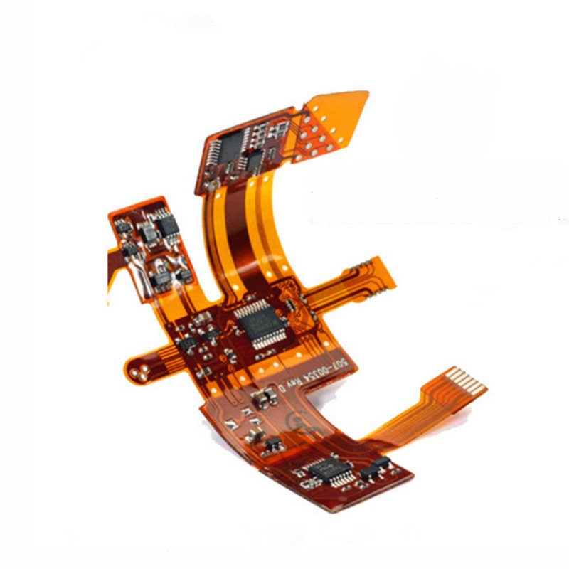
| FPC | 5-10 Days | 7-14 Days | Flexible Circuits, Mobile Devices |
| High-Frequency | 7-15 Days | 5-10 Days | Communication Base Stations, RF Modules |
PCB rapid prototyping
——We provide PCB rapid prototyping service with 24-hour turnaround
- For expedited PCB prototyping, we can deliver simple double-sided PCBs in as fast as 24 hours, and multi-layer boards within 48 hours.
- Each prototype undergoes at least five quality inspection processes, with trace accuracy controlled within ±0.01mm and the defect rate kept below 0.3%.
- We offer expedited small-batch PCB prototyping starting from 1 piece, meeting clients' pre-production needs and reducing upfront costs.
- For rush PCB prototyping orders, our engineers provide 1-on-1 technical support and complete DFM analysis within 2 hours.
PCB Prototype Specifications
| Specifications | Details |
|---|---|
| Board Type: | Single, Double, 4, 6, 8, 10+ layers. Max Size: 620 x 1100mm |
| Materials: | FR-4、Aluminum、PTFE/Teflon、Rogers series、Taconic series、Arlon series、Nelco series、Ceramic |
| Surface Finishes: | HASL、ENIG、OSP、HDI、High multi-layer blind&buried PCB、Backplane、Heavy copper power PCB、Backdrill、Immersion Silver |
| Layers: | 1-40 Layers |
| Thickness: | 0.8, 1.0, 1.2, 1.6 (standard), 2.0mm |
FAQ
1、What's the fastest Turnaround Time for PCB prototyping?
- Standard lead times: 2-layer (≤10 pcs) in 1-3days, 4-layer in 2-7 days,6,8 layer in 3-10 days,10+layer in 4-15 days.
- Expedited service: 2-layer (≤10 pcs) in 24hours, 4-layer in 48 hours,8+layer in 3-5 days.
specialized processes (e.g., impedance control, high-frequency materials) may take up to 48 hours.
Place orders 1-2 days in advance with clear delivery time specifications.
2、What is the price for PCB prototyping?
Base Cost: Things like type of substrate material—FR-4 vs. a high-frequency material, number of layers (2, 4, 8), thickness, size.
Processing Fees: Basic “base item” processes are cheapest; additional processes are costs on top of basic quotes. Fees for surface treatments such as electroless nickel plating, hot air leveling, organic solder mask, impedance control, blind/buried vias, custom solder mask colors are added to pricing.
Rush Fees: About 20%-50% for 24-hour or 48-hour “get it out the door” service fees.
Prices differ from mfr. to mfr. depending on things like precision of equipment, grades of material, complexities of process, inspection.
3. What files do you need to provide for PCB prototyping?
PCB prototyping requires: Gerber production files in RS-274X, and Excellon drill files. You may also provide specifications (board material, thickness, surface finish, etc). For SMT assembly you will also need to provide coordinate files and a BOM list.
4、What kinds of panel thicknesses are available?
We offer all kinds of substrates in our PCB prototyping service. The standard FR-4 (TG135/TG150) is arguably the most widespread choice, while metal substrates like aluminum or copper boards are often used for heat dissipation purposes in LED lighting or power modules. Flexible PCBs (FPC) are bendable, allowing the adaptability needed for wearables, foldable screens, or anything with a smaller footprint. Prototyping FR-4 1.6mm is something I would recommend upfront since it will save you basically 30%-50% of materials costs and satisfy most of your testing.
Inquiry
Free existing samples or similar-function pcba or solutions for reference.
sales development:
- sales@huasunpcb.com
- +86-13826586481
Support
Professional one-stop service for PCBA from design to production.